
The strategy makes use of vapor to make tin transistors that work and final, serving to make low-cost, large-area electronics and higher OLED screens.
Researchers at Pohang College of Science and Expertise have developed a technique to make TFTs utilizing tin-halide perovskites. Their strategy makes use of thermal evaporation together with lead chloride (PbCl₂) as a response starter.
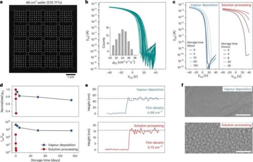
Based mostly on these steps, a technique was developed to manufacture tin perovskite TFTs. The technique makes use of vapor deposition to deposit PbCl₂, tin iodide (SnI₂), and cesium iodide (CsI) onto a substrate.

On this methodology, the mixture of those supplies kinds cesium-tin-iodide (CsSnI₃)-based perovskites, with PbCl₂ as the bottom layer. The chloride triggers solid-state reactions that convert the deposited precursors into perovskite movies. This course of additionally adjusts the outlet density to ranges appropriate to be used in transistor channel layers.
The ensuing p-channel transistors confirmed efficiency with gap mobilities of 33.8 cm²/V·s and on/off present ratios round 10⁸. These values are just like, and in some circumstances higher than, these of gadgets made utilizing solution-based strategies. In distinction, earlier makes an attempt at making perovskite transistors by way of deposition reported mobilities beneath 1 cm²/V·s, making them unfit to be used. The vapor-deposited transistors additionally confirmed stability, which helps sensible and scalable use.
Utilizing this methodology, the researchers made and examined transistors, evaluating them to transistors utilized in natural light-emitting diodes (OLEDs). Their gadgets outperformed IGZO-based oxide transistors utilized in OLED driving circuits.
The group believes that these p-type TFTs may assist OLEDs work higher and use much less energy. The research might also assist extra work on vapor deposition strategies for making tin-halide perovskite transistors at scale. In time, this work may result in large-area, low-cost VLSI electronics and stacked circuit designs.
Subsequent steps embody supplies engineering and machine integration. On the supplies aspect, the objective is to discover compositions that permit lower-temperature processing and management over machine traits comparable to turn-on voltage and hysteresis. On the appliance aspect, vapor deposition might permit vertical stacking of perovskite layers, resulting in circuit designs with out solvent-based photolithography. These instructions may broaden using perovskite-based electronics.
Reference: Youjin Reo et al, Vapour-deposited high-performance tin perovskite transistors, Nature Electronics (2025). DOI: 10.1038/s41928-025-01380-8.
