
Courtesy: Synopsys
Current developments in machine studying have resulted in enhancements in synthetic intelligence (AI), together with picture recognition, autonomous driving, and generative AI. These advances are primarily because of the capability to coach giant fashions on more and more advanced datasets, enabling higher studying and generalization in addition to the creation of bigger fashions. As datasets and mannequin sizes develop, there’s a requirement for extra highly effective and optimized computing clusters to assist the subsequent era of AI.
With greater than 25 years of expertise in delivering field-proven silicon IP options, we’re thrilled to companion with NVIDIA and the NVIDIA NVLink ecosystem to allow and speed up the creation of customized AI silicon. This strategic collaboration will leverage Synopsys’ experience in silicon IPs to help within the improvement of bespoke AI silicon, forming the muse for superior compute clusters aimed toward delivering the subsequent era of transformative AI experiences.
Compute challenges with bigger datasets and more and more giant AI fashions
Coaching trillion-parameter-plus fashions on giant datasets necessitates substantial computational sources, together with specialised accelerators akin to Graphics Processing Models (GPUs) and Tensor Processing Models (TPUs). AI computing clusters incorporate three important capabilities:
- Compute — applied utilizing processors and devoted accelerators.
- Reminiscence — applied as Excessive Bandwidth Reminiscence (HBM) or Double Information Charge (DDR) with digital reminiscence throughout the cluster for reminiscence semantics.
- Storage — applied as Strong State Drives (SSDs) that effectively switch knowledge from storage to processors and accelerators by way of Peripheral Part Interconnect Specific (PCIe)-based Community Interface Playing cards (NICs).
Retimers and switches represent the material that connects accelerators and processors. To boost the computational capabilities of the cluster, it’s mandatory to extend capability and bandwidth throughout all capabilities and interconnects.
Growing more and more subtle, multi-trillion-parameter fashions requires the whole cluster to be linked over a scale-up and scale-out community so it will possibly operate as a unified laptop.

Determine 1: A consultant compute cluster with scale-up and scale-out community.
Requirements-based IPs for actually interoperable compute clusters
The profitable deployment of next-generation computing clusters depends on silicon-verified interconnects that make the most of superior course of node know-how and assure interoperability. Standardized interconnects allow an interoperable, multi-vendor implementation of a cluster.
PCIe is a longtime customary for processor-to-accelerator interfaces, making certain interoperability amongst processors, NICs, retimers, and switches. Since 1992, the PCI-SIG has been defining Peripheral Part Interconnect (PCI) options, with PCIe now in its seventh era. The intensive historical past and widespread deployment of PCIe make sure that IP options profit from the silicon studying of earlier generations. Moreover, the whole ecosystem creating processors, retimers, switches, NICs, and SSDs possesses vital deployment expertise with PCIe know-how. Our full IP answer for PCIe 7.0 is constructed upon our expertise with greater than 3,000 PCIe designs, launched in June 2024 with endorsements from ecosystem companions akin to Intel, Rivos, Xconn, Microchip, Enfabrica, and Kandou.
When deploying educated fashions within the cloud, hyperscalers intention to proceed using their software program on customized processors that interface with varied forms of accelerators. For NVIDIA AI factories, NVLink Fusion offers one other methodology for connecting processors to GPUs.
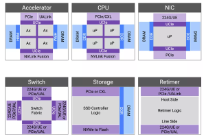
Determine 2: Elements and interconnects of a next-generation compute cluster.
Accelerators might be linked in varied configurations, affecting the effectivity of compute clusters. Scale-up requires reminiscence semantics for a digital reminiscence pool throughout the cluster, whereas scale-out includes connecting tens-of-thousands to hundreds-of-thousands of GPUs with layers of switching and congestion administration. Not like scale-up, scale-out is extra latency-tolerant and designed for bandwidth oversubscription to go well with AI mannequin knowledge parallelism. In December 2024, we launched our Extremely Accelerator Hyperlink (UALink) and Extremely Ethernet answer to attach accelerators effectively. The answer, which was publicly supported with quotes from AMD, Juniper and Tenstorrent, is predicated on silicon-proven 224G PHY and greater than 2,000 Ethernet designs.
Trillion-parameter fashions demand intensive reminiscence storage and excessive knowledge charges for low latency entry, necessitating elevated reminiscence bandwidth and complete capability. HBM offers each substantial capability and excessive bandwidth. Our HBM4 IP represents the sixth era of HBM know-how, providing pin bandwidths as much as 12 Gbps, which ends up in an total interface bandwidth exceeding 3 TBps.
Co-packaged multi-die aggregation not solely enhances compute throughput by overcoming the constraints of superior fabrication processes but in addition facilitates the combination of optical interconnects by rising Co-Packaged Optical (CPO) applied sciences. Since 2022, we now have been creating linear electro-optical (EO) interfaces to create energy-efficient EO hyperlinks. The Common Chiplet Interconnect Specific (UCIe) customary has offered a well-defined path for multi-vendor interoperability. In collaboration with Intel in 2023, we efficiently demonstrated the primary UCIe-connected, chiplet-based take a look at chip.
Multi-die integration poses challenges for warmth dissipation, doubtlessly impacting temperature-sensitive photonic parts or inflicting thermal runaway. Our complete multi-die answer, together with Die-to-Die IP, HBM IP, and 3DIC Compiler for system-in-package integration, offers a dependable and strong multi-die implementation.
Adopting well-established and extensively validated IP options throughout vital interconnects – from processor-accelerator interfaces to superior multi-die architectures and HBM – mitigates the dangers related to customized design and integration. Pre-verified IPs streamline the design and verification course of, speed up timelines, and in the end pave the way in which for profitable first-pass silicon, enabling the fast deployment of revolutionary and interoperable compute clusters.
