
- New license settlement enabling the proliferation of metasurface optics throughout high-volume client, automotive and industrial markets: from smartphone purposes like biometrics, LIDAR and digicam help, to robotics, gesture recognition, or object detection.
- The settlement broadens ST’s functionality to make use of Metalenz IP to provide superior metasurface optics whereas leveraging ST’s distinctive expertise and manufacturing platform combining 300mm semiconductor and optics manufacturing, take a look at and qualification.
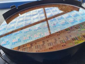
STMicroelectronics, a world semiconductor chief serving prospects throughout the spectrum of electronics purposes and Metalenz, the pioneer of metasurface optics, introduced a brand new license settlement. The settlement broadens ST’s functionality to make use of Metalenz IP to provide superior metasurface optics whereas leveraging ST’s distinctive expertise and manufacturing platform combining 300mm semiconductor and optics manufacturing, take a look at and qualification.
“STMicroelectronics is the distinctive provider in the marketplace providing a groundbreaking mixture of optics and semiconductor expertise. Since 2022, we now have shipped effectively over 140 million metasurface optics and FlightSense™ modules utilizing Metalenz IP. The brand new license settlement with Metalenz bolsters our expertise management in client, industrial and automotive segments, and can allow new alternatives from smartphone purposes like biometrics, LIDAR and digicam help, to robotics, gesture recognition, or object detection,” underlined Alexandre Balmefrezol, Govt Vice President and Basic Supervisor of STMicroelectronics’s Imaging Sub-Group. “Our distinctive mannequin, processing optical expertise in our 300mm semiconductor fab, ensures excessive precision, cost-effectiveness, and scalability to fulfill the requests of our prospects for high-volume, complicated purposes.”
“Our settlement with STMicroelectronics has the potential to additional fast-track the adoption of metasurfaces from their origins at Harvard to adoption by market main client electronics firms,” stated Rob Devlin, co-founder and CEO of Metalenz. “By enabling the shift of optics manufacturing into semiconductor manufacturing, this settlement has the likelihood to additional redefine the sensing ecosystem. As use circumstances for 3D sensing proceed to broaden, ST’s expertise management out there along with our IP management solidifies ST and Metalenz because the dominant forces within the emergent metasurface market we created.”
The brand new license settlement goals to handle the rising market alternative for metasurface optics projected to expertise vital progress to achieve $2B by 2029*; largely pushed by the trade’s position in rising show and imaging purposes. (*Yole Group, Optical Metasurfaces, 2024 report)
