

A brand new metalens makes cameras slimmer with out dropping clear view or monitoring. It might change how telephones and gadgets look subsequent.
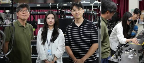
Samsung Electronics and Pohang College of Science and Know-how (POSTECH) have developed a metalens for eye cameras, enabling thinner XR gadgets and decreasing the peak of smartphone digital camera modules. The change cuts digital camera thickness by 20% from 2.0 mm to 1.6 mm whereas conserving gaze monitoring, iris feature-point recognition, and a 120-degree subject of view. Modulation switch perform (MTF) efficiency improved from 50% to 72%.
The staff overcame technical challenges that had blocked the commercialization of metalenses. They demonstrated mild diffraction utilizing a two-thirds wavelength section delay as an alternative of the total wavelength usually required. This was performed by arranging nanostructures in a supercell that saved a continuing section gradient and secure wavefront within the far subject.
Since section delay is ready by nanostructure width and peak, the diminished requirement lowered the side ratio from about 1:10 to 1:5. This decreased construction peak with out reducing optical efficiency, making fabrication simpler, decreasing defects, bettering stability, and rising manufacturing effectivity and price competitiveness.
A metalens is a skinny lens that shapes mild via nanoscale buildings on a flat floor as an alternative of curved surfaces utilized in conventional lenses. These buildings are thinner than a human hair, making them helpful for small optical gadgets. In conventional designs, reaching a one-wavelength section delay requires constructing tens of hundreds of thousands of slender, tall nanostructures, that are laborious to provide at scale and inclined to break.
On this examine, the staff utilized the two-thirds wavelength section delay strategy to construct an infrared eye digital camera for XR gadgets. Regardless of its diminished thickness and weight, the digital camera delivered pupil monitoring and iris sample recognition.
Samsung’s position within the venture was to indicate the potential of next-generation photonic gadgets and create alternatives for product differentiation. The analysis lined the method from idea to implementation and validation.
The know-how is predicted to develop into the seen mild spectrum, serving to scale back smartphone digital camera protrusion and enabling the miniaturization of imaging sensor techniques, opening new paths for gadget differentiation.
