

Within the late Nineteen Eighties and Nineties, the Recreation Boy redefined handheld leisure. With its chunky buttons, monochrome display, and pocket-sized design, it developed from a toy right into a cultural icon (see Fig. 1). For a lot of, it was the primary glimpse into moveable electronics, sparking curiosity about gaming and the know-how behind it. Many years later, the Recreation Boy continues to captivate retro players, engineers, and hobbyists, inspiring makers and hackers to reinvent its legacy.
Constructing on that legacy, the Smallest Transportable Recreation Boy Retro Console and Wi-Fi Hacking Machine (see Fig. 1) unites retro gaming attraction with trendy embedded know-how. Powered by the ESP12F Wi-Fi module (ESP8266), it permits retro-style gaming, Wi-Fi scanning, deauthentication, and Wi-Fi penetration testing. Its compact 4.5cm spherical PCB packs all necessities—an LDO regulator, capacitors, resistors, a battery connector with energy swap, and tactile management buttons.
Show choices embrace an OLED SSD1306 for a traditional 90s look or a TFT LCD for contemporary visuals. Supported by open supply libraries, the system permits growth of customized video games or deployment of prebuilt hacking instruments, making it a flexible, retro-inspired, future-ready system for makers and safety researchers.

The ESP12F chip delivers the processing energy required for operating Recreation Boy video games whereas supporting Wi-Fi hacking, making it perfect for dual-use designs. It offers ample I/O, reminiscence, and a compact footprint that aligns with system necessities.
The design additionally presents flexibility in show choices. Customers can choose an OLED show (over I²C) or a color show such because the ST7789V round-edge, GC9A01, or some other appropriate module. Each sorts can function concurrently, with OLED on I²C and color shows on SPI. Energy regulation is managed by an LDO regulator, guaranteeing secure operation throughout all elements.

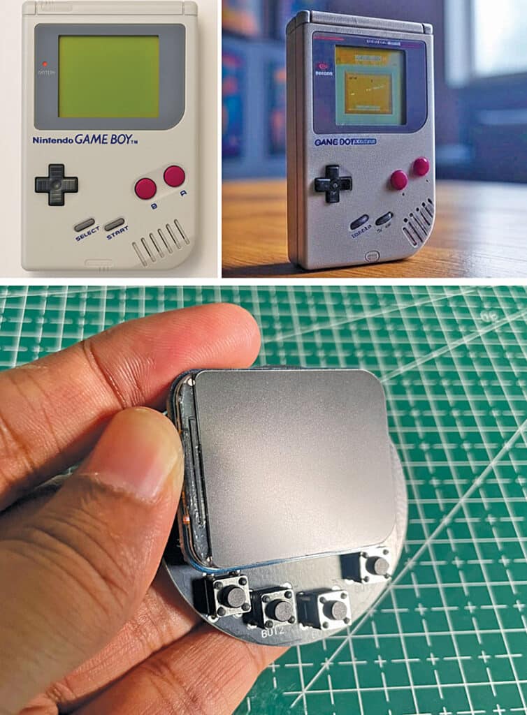
All elements are SMD to keep up a small, compact kind issue, with solely the buttons utilizing through-hole footprints. Fig. 1 exhibits the writer’s prototype, whereas Fig. 2 compares the market-available Recreation Boy with the writer’s design. Required elements are listed within the Invoice of Supplies (Desk 1).
| Desk 1: Invoice of Supplies | |||||
| Title | Designator | Footprint | Amount | Producer Half | Producer |
| 6X6-PUSH BUTTON COPY | BUT1, BUT2, BUT3, BUT4 | 6X6-PUSH BUTTON |
4 | ||
| 100nF | C1 | C0402 | 1 | GRM155R71H104KE14D | muRata |
| 1µF | C2, C3 | C0402 | 2 | CL05A105KP5NNNC | SAMSUNG |
| SM02B-SRSS-TB (LF)(SN) | CN1 | CONN-SMD_2P-P1.00_SM02B-SRSS-TB-LF-SN | 1 | SM02B-SRSS-TB (LF)(SN) | JST |
| OLED DISPLAY | LCD1 | SSD1306-OLED-128X64-I2C | 1 | ||
| ESP-12F | MOD1 | WIFIM-SMD_ESP-12F-ESP8266MOD | 1 | ESP-12F (ESP8266MOD) | Ai-Thinker |
| 10kΩ | R1, R2 | R0603 | 2 | RC0603FR-0710KL | YAGEO |
| MK-11C04-G013 | SW2 | SW-SMD_MK-11C04-G013 | 1 | MK-11C04-G013 | G-Change |
| St7789v | U1 | 1.28-inch Spherical Edge Show | 1 | 19192 | Waveshare |
| USB 2.0 Solder Pad | U3 | USB SOLDER PADS | 1 | ||
| SK6018CD4-28 | U4 | DFN-4_L1.0-W1.0-P0.65-BL-EP | 1 | SK6018CD4-28 | suntek |
Design
The first requirement of the system is an influence provide able to working the whole system. The ESP12F helps an working voltage vary of three.0V to three.3V, and the show operates throughout the identical vary. Due to this fact, a 3.3V regulated provide is required to offer a secure voltage, no matter whether or not the enter supply is a 3.7V Li-ion/LiPo battery, a 5V or 7V battery, or USB 5V energy. The regulator ensures a clear and secure 3.3V output for the whole system.
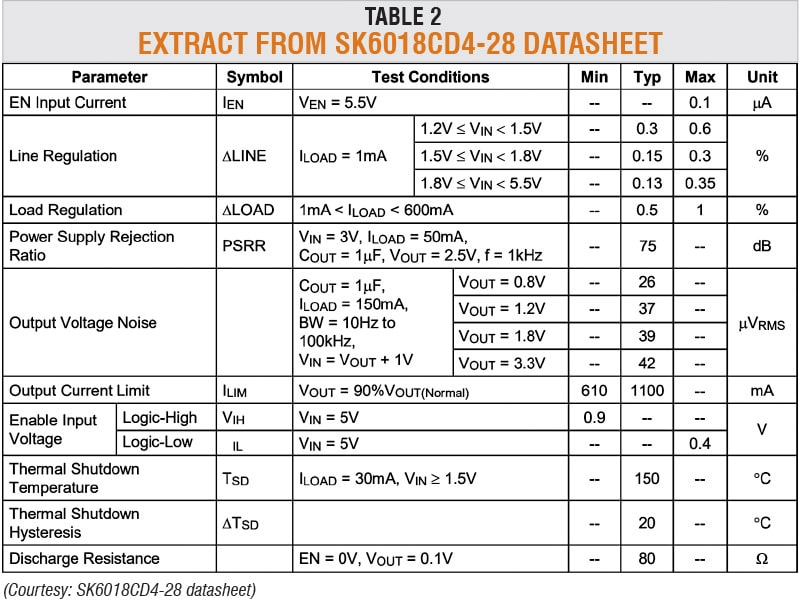
An LDO regulator is employed for this objective. Whereas a typical AMS1117-3.3 or comparable 3.3V LDO may very well be used, the SK6018CD4-28 was chosen to keep up a compact kind issue. It is available in a really small DFN-4 (1mm×1mm) package deal, saving PCB area. The datasheet specifies an enter voltage vary of 1.2V to five.5V, delivering an output present of as much as 600mA (VIN ≥2.3V with EN enabled). That is ample to energy the ESP12F throughout peak processing and Wi-Fi transmission, in addition to the show module. Desk 2 exhibits an extract from the SK6018CD4-28 datasheet.
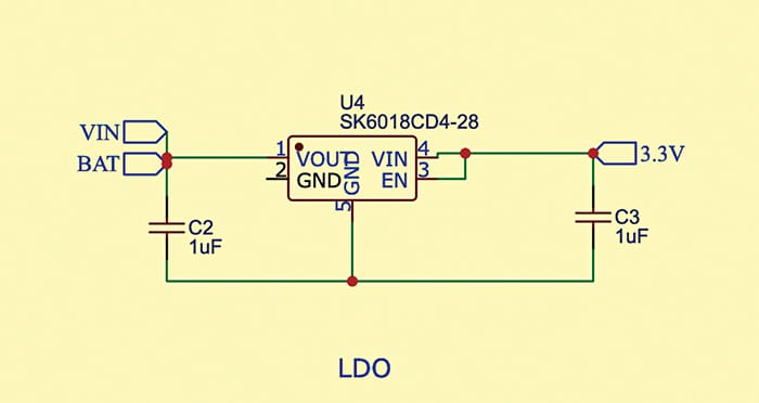
The LDO requires two 1µF ceramic capacitors (one between VIN and GND, and one between VOUT and GND) to make sure stability and correct filtering. SMD ceramic capacitors are used to keep up compactness. Consult with Fig. 3 for the LDO voltage regulator circuit.
Recreation Boy Core ESP12F Design
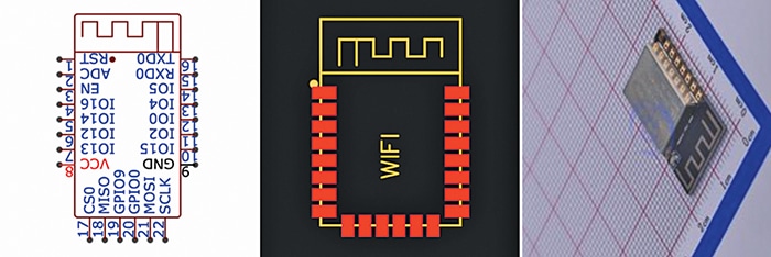
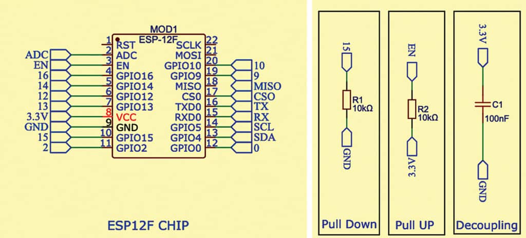
In response to the datasheet, the ESP12F offers 22 GPIO pins, together with three strapping pins (GPIO0, GPIO2, and GPIO15) that decide the boot configuration. For regular boot mode, GPIO15 have to be pulled to GND through a resistor. Throughout programming or firmware add, GPIO0 have to be pulled low; a jumper is supplied to pressure this pin low solely throughout add, whereas it stays pulled excessive throughout regular operation. The EN (CH_PD) pin is pulled as much as VCC through a resistor to maintain the chip enabled.
For Steady Booting
To make sure secure booting, observe these steps:
- Pull GPIO15 all the way down to GND for regular boot utilizing R1 (10kΩ).
- Pull GPIO0 low solely throughout programming to allow firmware add; in regular operation, it stays excessive.
- Maintain GPIO2 pulled up to make sure the right boot configuration.
- Pull EN (CH_PD) as much as 3.3V utilizing R2 (10kΩ) to maintain the chip enabled.
A decoupling capacitor, C1 (100nF), needs to be positioned near VCC and GND to filter high-frequency noise and stabilise the facility rail throughout Wi-Fi transmission bursts. The module options devoted VCC (3.3V) and GND pins. With acceptable pull-up, pull-down, and decoupling networks, the ESP12F operates reliably because the core of the moveable system.
Peripheral connections use the remaining GPIOs and are routed for both an OLED show (I²C: SDA, SCL) or SPI color shows (MOSI, SCLK, CS, DC) together with button inputs for person management. Fig. 4 exhibits the ESP12F footprint and pinout, and Fig. 5 exhibits the chip configuration.
Full Circuit
Fig. 6 exhibits the entire circuit diagram of the moveable Recreation Boy and Wi‑Fi hacking system. For readability, the circuit is split into subsections.
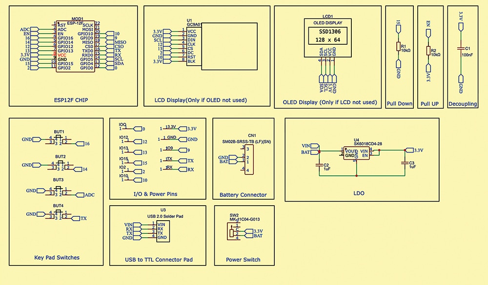
Keypad buttons
4 tactile push-buttons present sport controls, menu choice, and primary UI navigation. Buttons are mapped to out there GPIO pins; the design is expandable, as an example, through an I²C-based contact keypad. Consult with Fig. 7 for the entire circuit.
Battery connector
A SM02B-SRSS-TB connector accepts a single-cell Li‑ion or LiPo battery. The connector routes BAT and GND to the LDO regulator, offering a secure 3.3V provide to the ESP12F and the show, supporting a compact, wearable kind issue.
USB to TTL programming pad
A USB 2.0 solder pad exposes VIN, RX, TX, and GND for connection to an exterior USB-to-TTL adaptor (FTDI/CP2102/CH340), enabling firmware flashing and debugging with out extra {hardware}.
Energy swap
A slide swap (SW2–MK-51C04-G013) is positioned between the three.3V regulator output and the battery enter to disconnect the battery when not in use, thereby stopping pointless drain.
I/O and energy pins
Unused GPIOs (IO0, IO2, IO9, IO10, IO12, IO13, IO15, TX, RX) plus 3.3V and GND are routed to a header for enlargement with exterior modules, sensors, or extra controls. This extends performance past gaming to prototyping and IoT functions.
PCB Design
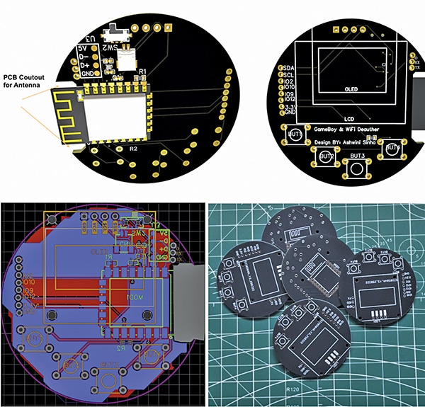
The ESP12F module is positioned on the underside layer with the USB footprint and discrete elements; the OLED header is on the highest aspect. SPI headers for a color show are positioned to the left, and tactile buttons sit beneath the show. When Wi‑Fi is required, the ESP12F antenna have to be positioned outward with a PCB cutout to make sure optimum sign efficiency and scale back interference from surrounding elements. A revised structure contains an antenna cutout and correct module placement. Fig. 7 illustrates the PCB structure with the antenna cutout in addition to the manufactured PCB.
SMT Soldering
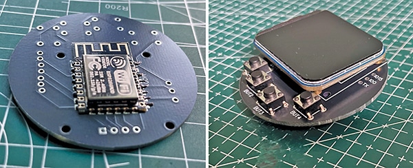
After PCB fabrication, carry out SMT soldering, set up the tactile buttons, and mount the show. The system is then prepared for testing. Fig. 8 exhibits the ESP12F SMT placement and the assembled board.
Software program
Customized video games might be developed and deployed to the system. Instance recreations embrace Flappy Fowl, Pong, and Tetris. Supply code and sources can be found through the QR code on this article.
Setup steps:
- Set up the TFT_eSPI library and the ESP8266 board package deal within the Arduino IDE
- Configure User_Setup.h for the chosen show (see [TFT_eSPI documentation](https://doc-tft-espi.readthedocs.io/beginning))
- Place the board in obtain mode by connecting GPIO0 to GND. Join RX, TX, and energy through the USB solder pads to an FTDI adaptor, then add the sketch
- Optionally, allow OTA updates to add video games over Wi‑Fi
Testing
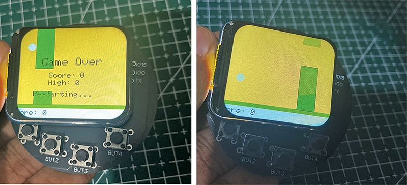
After importing the code and assembling the system, join the battery and take a look at the video games. The system will also be repurposed with Wi‑Fi Deauther firmware or different Wi‑Fi instruments for experimentation. Customers should observe relevant legal guidelines and moral tips. Fig. 10 exhibits the console operating a sport.
Bonus: You may watch the video of the tutorial for this DIY undertaking beneath:
