

From powering smartphones to enabling AI, semiconductors drive the fashionable financial system, and India is racing to construct a resilient chip ecosystem to affix the worldwide leaders. What lies forward regardless of challenges?
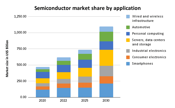
Semiconductors, or chips, are tiny digital units with hundreds of thousands or billions of transistors that course of information and handle electrical currents. Key classes embody reminiscence, microprocessors, sensors, and optoelectronics. These chips energy the whole lot from smartphones to superior healthcare programs and autonomous autos. Semiconductors are essential to rising applied sciences like 5G, synthetic intelligence (AI), and the Web of Issues (IoT), driving a cycle of innovation in pace, effectivity, and performance. Their manufacturing requires complicated expertise, heavy funding, and expert manpower. The worldwide semiconductor market is projected to achieve US$1 trillion by 2030.
Semiconductors at the moment are as important as oil, driving the fashionable information financial system. Dominated by international locations like Taiwan, China, South Korea, Japan, and the US (US), the sector is extremely concentrated, creating world dependence. Provide chain disruptions from COVID-19, geopolitical tensions, and commerce conflicts have prompted nations to develop impartial semiconductor ecosystems. India, recognising the strategic significance, is engaged on an bold plan to ascertain a resilient and sustainable semiconductor {industry}.

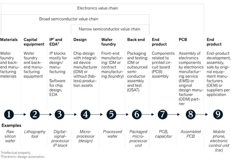
World semiconductor provide chain: an summary
The worldwide semiconductor provide chain is a extremely intricate community involving numerous gamers in design, manufacturing, and distribution. It additionally integrates mental property (IP) administration, materials recycling, waste disposal, and sustainability efforts. Broadly, the availability chain may be divided into 4 key levels: chip design, fabrication, meeting, packaging and testing, and distribution. Every stage is interdependent, that means disruptions can have a cascading influence throughout all the course of. Efficient coordination at each degree is significant to make sure the well timed and environment friendly supply of chips to end-users.

Chip design:
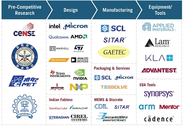
Chip design is a multidisciplinary course of that includes requirement evaluation, specification formulation, architectural design, logic improvement, and masks creation. Whereas some corporations design chips in-house, others outsource this operate to ‘fabless’ corporations, which focus solely on design and never fabrication. The US, Japan, China, and the UK lead in chip design, with India rising as a big hub for analysis and improvement (R&D) and innovation. India is house to twenty% of the world’s semiconductor design engineers, and a lot of design patents are registered right here. Design represents 15–20% of the availability chain worth.

)
Chip fabrication:
Chip fabrication begins with making ready high-purity silicon wafers, that are then sliced into skinny, polished wafers. The method contains photolithography, etching, doping, and materials deposition to kind the intricate circuit patterns. This multi-step course of happens in ultra-clean fabrication vegetation, often known as ‘fabs.’ Fabs use superior methods like excessive ultraviolet (EUV) lithography to create nanometre-scale options. Taiwan Semiconductor Manufacturing Firm (TSMC) and South Korea’s Samsung are world leaders on this area, with fabrication accounting for 35–40% of the availability chain worth.

https://www.nist.gov/)

Chip testing, meeting, and packaging (TAP):
After fabrication, wafers are diced into particular person chips, often known as ‘dies,’ and mounted onto frames for testing and packaging. Testing ensures chips meet specs and high quality requirements. Main gamers on this stage embody China, Taiwan, South Korea, and Singapore, whereas India’s aggressive labour pressure positions it to develop into a big participant sooner or later. TAP accounts for 15–20% of the availability chain worth.
Chip distribution:
Chips are distributed to producers for gadget integration or on to end-users. The US, Canada, China, and Taiwan play main roles in distribution, whereas India’s market continues to develop. This phase captures 5–10% of the availability chain worth, with end-users accounting for 15–20%.
Key gamers within the world provide chain
The semiconductor {industry} is dominated by key gamers throughout numerous levels of the availability chain. TSMC leads in superior foundry providers. Samsung performs a serious function in chips for information centres, automotive programs, IoT units, and wearables. Intel is famend for microprocessors, whereas Qualcomm powers wi-fi communication applied sciences in smartphones and automotive programs. NVIDIA is a pacesetter in graphics processing models (GPUs) for gaming and AI computing platforms. Superior Micro Gadgets (AMD) is a fabless firm specialising in processors. Broadcom innovates in networking, storage, and broadband options, whereas Micron Expertise excels in reminiscence and information storage. JUSDA gives logistics options together with warehousing and provide chain optimisation.
The challenges
The worldwide semiconductor provide chain faces a number of challenges that disrupt its stability. These embody pandemics, geopolitical tensions, commerce disputes, and pure disasters, all of which might trigger vital delays and shortages.
Technological Developments:
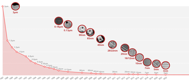
The continual push for technological developments ends in shorter product lifecycles, with 2nm node expertise, for instance, requiring investments of over $20 billion in EUV gear.
https://www.tsmc.com/english/dedicatedFoundry/expertise/logic/l_5nm)
Pure disasters and pandemics:
Pure disasters like floods, earthquakes, and pandemics have proven how susceptible the availability chain is. The COVID-19 pandemic and different disruptions in Taiwan, Malaysia, and Japan have severely impacted the availability chain.
Geopolitical tensions:
Commerce restrictions and export controls, particularly resulting from geopolitical conflicts, prohibit entry to essential supplies for semiconductor manufacturing, resulting in world provide chain disruptions.
Workforce shortages and ability gaps:
The speedy enlargement of the semiconductor sector has created a scarcity of expert manpower. Many international locations battle to fulfill demand for experience, requiring funding in workforce improvement by means of industry-academia partnerships.
Manufacturing unit slowdowns and shutdowns:
Incidents like labour strikes or accidents in factories, akin to these in Renesas Electronics and ASML, can halt manufacturing, affecting provide chains.
Weak transport routes:
A good portion of semiconductors is transported by way of sea routes, making provide chains susceptible to disruptions in essential maritime passages, such because the Suez Canal.
Environmental sustainability:
Semiconductor manufacturing is resource-intensive, requiring huge quantities of ultra-pure water, secure electrical energy, and dangerous chemical substances. Rising issues over the environmental influence demand funding in sustainable practices.
India’s semiconductor pursuit
India’s journey in direction of semiconductor self-sufficiency started in 1954 with the institution of Bharat Electronics Restricted (BEL) and Semiconductor Advanced Restricted (SCL). Whereas early efforts confronted challenges akin to a hearth at SCL and restricted funding, the nation has since made notable progress. In 1985, Gateway Design Automation (GDA) introduced semiconductor design operations to India, additional accelerating the nation’s function in chip design. By the late Nineties, India had develop into house to design centres of main corporations like Texas Devices and ST Microelectronics.
Regardless of setbacks, akin to excessive import duties and an absence of incentives, India is shifting from being a ‘chip-taker’ to a ‘chip-maker.’ The nation is specializing in attracting world semiconductor giants to arrange manufacturing services, whereas capitalising on its strengths in chip design. Authorities initiatives, together with the Nationwide Coverage on Electronics (NPE) 2019, the India Semiconductor Mission (ISM), and schemes like PLI and DLI, purpose to foster innovation, entice funding, and develop a talented workforce.
India’s technique additionally contains the ‘Chips to Startup’ programme, which can encourage home semiconductor manufacturing and place India as a key participant in world semiconductor provide chains. The imaginative and prescient is evident: India goals to diversify and strengthen the worldwide provide chain whereas rising as a pacesetter in chip manufacturing.
| Initiative | Key particulars |
| Nationwide Coverage on Electronics (NPE 2019) | Goals to make India a worldwide hub for ESDM with a goal of $400 billion turnover by 2025. Focuses on growing core elements, akin to chipsets, and fostering a globally aggressive setting. |
| India Semiconductor Mission (ISM) | A ₹760 billion initiative geared toward making a sustainable semiconductor ecosystem. Helps organising semiconductor fabrication, meeting, testing, and packaging models throughout India. |
| Manufacturing Linked Incentive (PLI) Scheme | A ₹760 billion scheme providing incentives for semiconductor manufacturing, with a give attention to attracting world investments in manufacturing models for elements like shows, photo voltaic cells, and others. |
| Design Linked Incentive (DLI) Scheme | Goals to advertise semiconductor design capabilities in India. The scheme allocates nearly ₹8.03 billion for 23 authorised initiatives, supporting prototyping and commercialisation of semiconductor designs. |
| Chips to Startup (C2S) Programme | A ₹30 billion initiative to nurture the semiconductor ecosystem by supporting startups, incubation, abilities improvement, and analysis. Focuses on fostering innovation and entrepreneurship within the semiconductor house. |
World collaborations and industrial initiatives
India’s semiconductor technique closely depends on collaborations with key international locations and stakeholders to construct a strong ecosystem. Partnerships with international locations such because the US, Japan, Singapore, and Taiwan play a pivotal function in enhancing India’s manufacturing and design capabilities.
- Japan is helping India with superior supplies, gear, and expertise, important for enhancing the manufacturing infrastructure.
- Taiwan, a worldwide chief in semiconductor manufacturing, helps arrange fabrication models and develop a extremely expert workforce in India.
- Singapore is partnering with India to reinforce its capabilities in semiconductor design, testing, and packaging.
- The US and India have established the Initiative on Crucial and Rising Applied sciences (iCET), aiming to strengthen cooperation in important expertise areas, together with semiconductors.
These collaborations span each stage of the semiconductor worth chain, from chip design to fabrication and packaging.
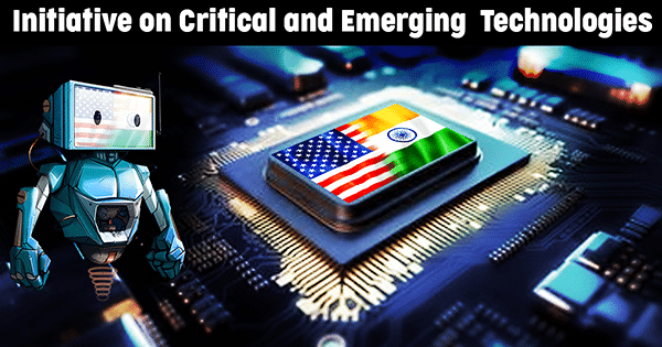
| Launched in January 2023 by India and the U.S., iCET strengthens cooperation in semiconductors, AI, quantum tech, house, telecom, and defence. It promotes joint R&D, provide chain resilience, public-private partnerships, and expertise alternate, aiming to place each nations as world tech leaders in an open, safe, and trusted innovation ecosystem. |
https://www.wrightresearch.in/)
Industrial initiatives in India
India can also be witnessing large-scale industrial initiatives, with vital investments from each home and worldwide gamers. These investments are serving to India set up state-of-the-art semiconductor manufacturing and testing services.
- Tata Electronics (TEPL) is collaborating with Taiwan’s Powerchip Semiconductor Manufacturing Company (PSMC) to construct India’s first AI-enabled fab in Dholera, Gujarat, with an funding of ₹910 billion. The fab could have a capability of fifty,000 wafers per thirty days, manufacturing chips for energy administration, show drivers, microcontroller models (MCUs), and high-performance computing logic.
- Tata Group is organising a ₹270 billion semiconductor meeting and testing facility in Assam, with a deliberate output of 15 billion chips yearly by 2025.
- Kaynes Expertise is establishing a ₹33 billion facility in Gujarat to fabricate microcontrollers and energy administration chips, with a capability of 6 million chips per day.
- Adani Group, in partnership with Israeli agency Tower Semiconductors, is investing $10 billion to arrange a chip manufacturing facility in Maharashtra, with a capability of 80,000 wafers per thirty days, set to be operational by 2027.
- CG Energy and Industrial Options has fashioned a JV with Renesas Electronics and Stars Microelectronics to arrange an outsourced meeting and testing (OSAT) facility in Sanand, Gujarat, with a ₹76 billion funding, focusing on 15 million models per day.
- Tarq Semiconductors, part of the Hiranandani Group, is organising an meeting, testing, marking, and packaging (ATMP) facility in Uttar Pradesh with Yotta Tech Providers.
- AMD has established a big design centre in Bengaluru, centered on growing high-performance CPUs, GPUs, and different semiconductor options.
These initiatives are positioning India as a rising participant within the semiconductor manufacturing house.
The function of Indian startups
India is house to over 100 semiconductor startups concentrated in expertise hubs like Bengaluru, Hyderabad, Chennai, and Pune. These startups are driving innovation in chip design, embedded programs, and AI-driven architectures. Notable startups embody:
- Signalchip, a pioneer in indigenous telecom chip improvement.
- Sankhya Labs specialises in wi-fi communication and software-defined radios for each business and defence functions.
- Mindgrove Applied sciences focuses on AI-driven chip design and energy-efficient options.
- Steradian Semiconductors excels in radar chip design for superior driver-assistance programs (ADAS) and autonomous autos.
However the hurdles…
Whereas India is making vital strides within the semiconductor sector, a number of challenges stay:
- Excessive funding: Establishing a contemporary semiconductor fab facility prices $25–30 billion. With speedy technological developments, these services require steady upgrades, making it a high-risk, capital-intensive {industry}.
- Scarcity of expert workforce: India faces a big expertise hole, with a projected scarcity of over 200,000 semiconductor specialists within the coming years. Constructing a talented workforce would require long-term funding in training, worldwide partnerships, and educational collaborations.
- Infrastructure limitations: Semiconductor fabs require subtle infrastructure, together with ultra-clean environments, managed temperatures, high-power stability, and huge portions of ultra-pure water. Securing the mandatory infrastructure and land for these services is a big logistical and monetary problem.
- World competitors: India is coming into the semiconductor race whereas competing in opposition to well-established gamers just like the US, which has dedicated $52 billion below the CHIPS and Science Act, and the EU, which goals to safe 20% of the worldwide market share by 2030.
India must proceed its push for investments, give attention to infrastructure improvement, and enhance its home marketplace for semiconductors to stay aggressive.
Trying on the future
The challenges however, India’s semiconductor ambitions are gaining traction. The federal government’s PLI and DLI schemes are attracting world gamers to put money into India, whereas ongoing industrial collaborations are strengthening the nation’s place within the world semiconductor provide chain.
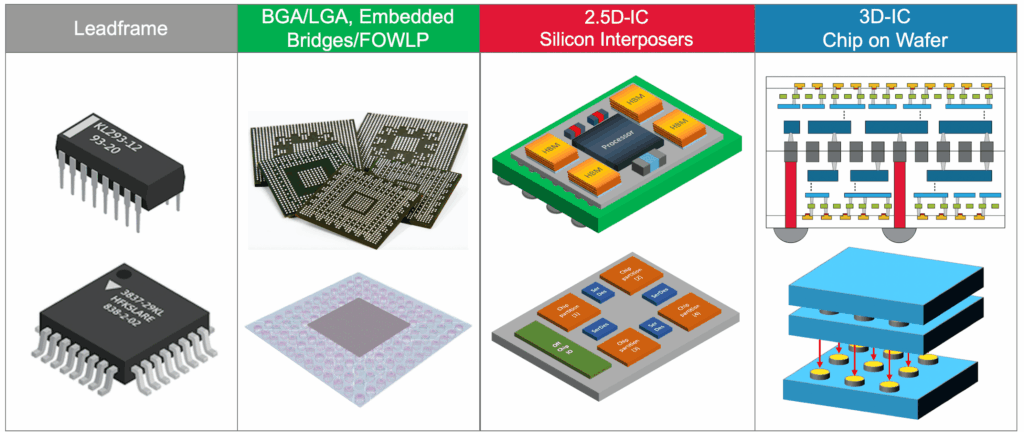
India should handle its infrastructure gaps, put money into coaching a big, expert workforce, and improve its R&D capabilities. By persevering with to construct worldwide partnerships, particularly in areas akin to chip design and 3D packaging, India has the potential to emerge as a worldwide chief within the semiconductor {industry}.
India’s journey towards semiconductor self-reliance requires sustained coverage assist, strategic collaborations, and a forward-looking strategy to beat present challenges and safe a robust place within the world market.
Authored By: Dr Deepak Halan.The creator is presently a professor at Jaipuria Institute of Administration, Noida.
