

The testing technique checks micro-LED wafers with out injury. It makes use of gentle probes and instruments to enhance yield, decrease prices, and pace up inspection.
Scientists at Tianjin College have created a brand new nondestructive testing technique for micro-LED wafers, utilizing a singular “soft-touch” method to handle a key business drawback.
Micro-LEDs are seen as a core know-how for future high-end shows. To keep up high quality and cut back restore prices, producers should obtain very excessive yields throughout wafer manufacturing. Nevertheless, reliably testing these wafers with out damaging them has lengthy been a technical barrier. This new method provides a potential path ahead.

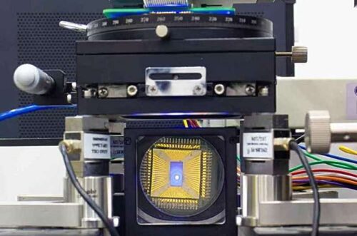
The analysis workforce has developed a versatile three-dimensional probe array that adapts to the microscopic floor of micro-LED wafers, making use of minimal strain—round 0.9 MPa—enabling electrical testing with out scratching or damaging the wafer. This soft-contact technique helps high-throughput testing whereas defending delicate surfaces.
The contact strain of those versatile probes is simply one-ten-thousandth that of conventional inflexible probes. This not solely preserves the wafer floor but in addition extends the probes’ service life. Even after a million contact cycles, the probes stay in authentic situation.
To enrich the probe array, the workforce designed a specialised measurement system that works in tandem with the versatile probes. Collectively, they provide a sensible resolution for course of monitoring and yield screening in micro-LED manufacturing.
This development addresses a long-standing hole in micro-LED electroluminescence testing and lays the groundwork for broader use in wafer inspection and biophotonics.
The know-how is now shifting towards commercialization at an area innovation park. It goals to ship a scalable, low-cost, and nondestructive testing platform for the increasing micro-LED sector, with potential to affect different areas of versatile electronics as effectively.
