

This development paves the way in which for mass-produced quantum methods—bringing quantum computing, sensing, and communication nearer to on a regular basis actuality.
For scalable quantum tech, researchers from Boston College, UC Berkeley, and Northwestern College have developed the first-ever digital–photonic–quantum chip constructed solely in a business semiconductor foundry. The chip, detailed in Nature Electronics, integrates quantum gentle sources with management electronics utilizing a mainstream 45-nanometer CMOS course of—bringing us nearer to mass-producible quantum gadgets.
This achievement merges quantum optics, photonics, and electronics on a single silicon platform. “It’s a small however important step in making repeatable, controllable quantum methods accessible via customary chip manufacturing,” stated BU’s Miloš Popović, senior writer of the examine.At its core, the chip acts as a quantum gentle manufacturing unit—utilizing microring resonators to generate streams of correlated photon pairs, key sources for quantum computing, communication, and sensing. Every chip consists of twelve such photon sources, working in parallel and stabilized via on-chip management logic and heaters.
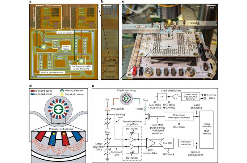
Sustaining the fragile photon-generation course of is notoriously tough. These microrings are extraordinarily delicate to warmth and fabrication variations—tiny adjustments can throw off your complete system. To fight this, the group embedded photodiodes contained in the resonators to observe their alignment in actual time. The chip’s management circuitry then self-adjusts, guaranteeing steady quantum gentle era whilst environmental situations fluctuate.

“This real-time stabilization of quantum sources on-chip is what makes this method scalable,” famous Northwestern Ph.D. scholar Anirudh Ramesh, who led the quantum measurements.What makes this much more groundbreaking is how the chip was made. Constructed utilizing GlobalFoundries’ business 45nm CMOS platform, the identical tech stack behind superior AI interconnect chips, it proves that quantum methods can share fabrication pipelines with on a regular basis electronics. “The problem was making photonics quantum-ready with out leaving the business course of window,” stated BU’s Imbert Wang.
UC Berkeley’s Daniel Kramnik, who led integration and packaging, summed it up: “We’ve proven that full quantum photonic methods—full with stabilization—may be in-built CMOS. That opens the door to large-scale deployment.” From safe quantum networks to next-gen sensing and computing, this chip may develop into the muse for the quantum-powered world forward.
