

What if a near-invisible layer of carbon was the very factor holding again your electrical automobile or good grid from turning into extra environment friendly? That’s precisely what Cornell researchers uncovered—and solved.

Think about designing highly effective new electronics—solely to seek out that generally they work superbly and generally by no means. That’s the dilemma scientists confronted with beta gallium oxide, a promising semiconductor touted for future electrical automobiles and energy grids. Regardless of its ultra-wide band hole and high-voltage potential, units constructed with it confirmed unpredictable efficiency. Why? Nobody had a transparent reply—till now.
Cornell researchers have pinpointed the hidden saboteur: a nanometer-thin layer of carbon contamination, typically left behind by fabrication strategies and even simply air. This microscopic barrier disrupts the essential metal-semiconductor interface, choking present movement within the very units meant to ship energy effectively.
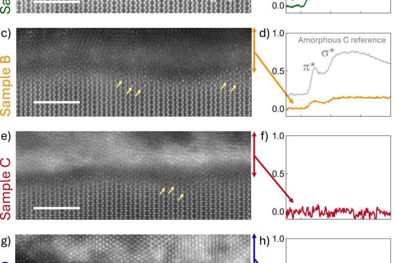
Doctoral researcher Naomi Pieczulewski and workforce went digging—on the atomic degree. Utilizing scanning transmission electron microscopy and superior imaging, they in contrast two commonplace methods of making use of metallic contacts to beta gallium oxide: the traditional lift-off technique and a metal-first method.
What they discovered was eye-opening. The lift-off samples confirmed residual carbon trapped between the metallic and semiconductor, a leftover from photoresist supplies. In the meantime, even the metal-first course of wasn’t immune—air publicity launched carbon too.
The workforce didn’t cease at analysis—they delivered a treatment. A one-hour UV-ozone remedy eliminated the carbon from lift-off samples, attaining an ultra-low contact resistance of simply 0.05 ohm-millimeters—among the many lowest ever reported for non-alloyed gallium oxide. A easy five-minute energetic oxygen course of cleaned the metal-first interfaces as properly.This collaborative effort united all seven co-PIs from the AFRL-Cornell ACCESS Heart, with contributions from Boise State and Micron by way of the Semiconductor Analysis Company.
“It is a step-change for ultra-wide bandgap electronics,” stated Pieczulewski. “It’s not flashy, however it’s foundational for transferring gallium oxide units from lab to real-world functions.”
