

A 3-layer cooler etched in silicon pulls warmth from dense chips whereas utilizing little energy, hinting that warmth could not restrict system dimension.
As digital units get smaller and extra highly effective, they launch extra warmth in much less quantity. This increased warmth density pushes system temperatures up and may injury inner components over time. That warmth is now a limiting issue for compact electronics utilized in computing, communication, protection, and client {hardware}.
To maintain units protected, engineers use thermal administration techniques. One method that’s thought-about promising for compact chips is microfluidic cooling, the place fluid is pushed by means of microscopic channels close to or inside an built-in circuit in order that warmth could be carried away. However many earlier microfluidic designs both fail to take away sufficient warmth at excessive energy density or require excessive pumping energy.
Researchers at Peking College and the Nationwide Key Laboratory of Superior Micro and Nano Manufacture Expertise have reported a brand new microfluidic cooling technique that may take away warmth extra successfully and with much less energy than many earlier methods. The work, revealed in Nature Electronics, describes a three-layer cooling system etched instantly right into a silicon substrate.
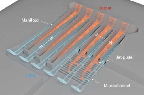
The highest layer is a tapered manifold that spreads water throughout the floor of a chip and ensures that every microchannel receives the identical quantity of coolant, creating uniform cooling. The center layer is the microjet layer, which has tiny nozzles that ship high-speed fluid streams instantly towards the chip floor to interrupt the thermal boundary the place warmth accumulates. The underside layer is a microchannel layer with sawtooth-shaped sidewalls that carries the heated coolant away.
The three layers are fabricated utilizing customary MEMS processes on the bottom of the silicon. In experiments, the system reached a coefficient of efficiency of 13,000 and eliminated a warmth flux of 1,000 W/cm² with a most temperature rise of 65 Ok. It additionally required solely 0.9 W/cm² of pumping energy and could be manufactured at scale utilizing current strategies.
This work by the Peking College crew exhibits a path to smaller, sturdy, and energy-efficient electronics by embedding warmth elimination buildings instantly into silicon. The design could be refined additional and examined throughout a broader class of compact units in future research.
