
New ultrathin diamond layers unfold warmth, making GaN chips cooler
As chips develop into smaller and sooner, the warmth they generate is changing into one of many greatest obstacles to efficiency. With transistor densities and energy calls for rising, conventional cooling strategies similar to followers, radiators, and liquid methods can not sustain.
Researchers at Stanford College have developed a brand new option to handle this warmth from contained in the chip itself utilizing ultra-thin diamond movies that unfold thermal vitality earlier than it turns into damaging.
The strategy permits the expansion of a micrometre-thick diamond layer instantly on semiconductor units at low temperatures. This inside warmth spreader helps management “sizzling spots,” which type when dense transistor exercise traps vitality in small areas. By dispersing warmth evenly throughout the chip, the know-how prevents overheating and reduces the necessity for big exterior cooling methods.
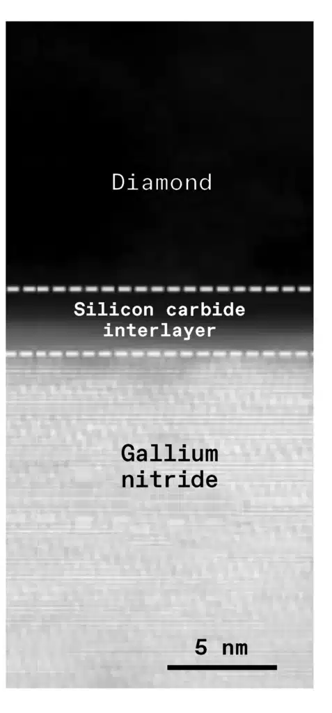
When utilized to gallium-nitride radio-frequency transistors, the diamond layer diminished working temperatures by as much as 70 °C, enhancing stability and energy dealing with. The researchers additionally discovered {that a} skinny silicon-carbide interface fashioned naturally between the diamond and semiconductor, creating an environment friendly bridge for warmth movement.
Diamond is among the most thermally conductive supplies, able to carrying warmth a number of occasions sooner than copper whereas remaining electrically insulating. Till just lately, diamond might be grown solely at round 1,000 °C, too sizzling for integration with silicon or gallium-nitride units.
The Stanford staff has achieved progress at about 400 °C, low sufficient to guard delicate interconnects and supplies utilized in superior chips.
The identical precept could be prolonged to three-dimensional chip stacks utilized in high-performance processors and AI accelerators. Skinny diamond sheets could be inserted between layers and linked by vertical warmth channels, permitting every layer to dissipate warmth successfully.
The challenge is being evaluated in collaboration with semiconductor producers similar to TSMC, Samsung, and Utilized Supplies. If built-in efficiently, the strategy may outline how next-generation computing {hardware} manages warmth as chip designs proceed to scale in energy and density.
