

Dealing with excessive stakes, but larger ambitions, Japan’s Rapidus presents the chip world with its first 2nm prototype chip. Will this large wager be capable to compete with the giants like TSMC?
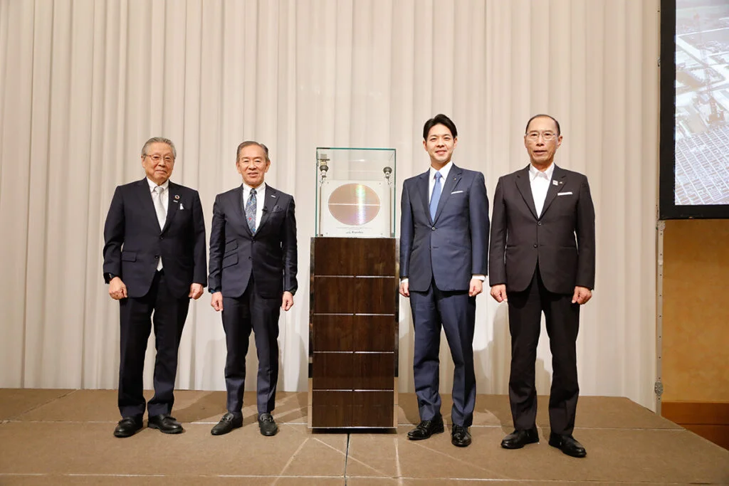
On July 18, at a press occasion in Chitose, Hokkaido, Japanese agency Rapidus Company confirmed that it had efficiently validated the nation’s first prototype chip constructed on cutting-edge 2-nanometre (nm) Gate-All-Round (GAA) transistor expertise.
This breakthrough marks a significant step for Japan in many years to re-enter the elite tier of superior semiconductor manufacturing; an trade it as soon as led, however lengthy ceded to rivals like Taiwan’s Taiwan Semiconductor Manufacturing Firm (TSMC) and South Korea’s Samsung. Backed by authorities assist and international partnerships, the prototype, maybe, indicators a method to shut the expertise hole and scale back dependency on international fabs amid escalating geopolitical dangers.
Rapidus stated it plans to supply chip design kits to clients by early 2026, with mass manufacturing focused for 2027, making it a possible fourth international participant within the race to commercialise 2nm chips.
A tech gamble with nationwide stakes
Based in August 2022, Rapidus was born out of Japan’s issues over the focus of superior semiconductor manufacturing in Taiwan. In accordance with a retrospective in Japan Ahead, the thought of constructing home 2nm chips originated from a proposal made by IBM to Tetsuro Higashi, former head of Tokyo Electron and now chairman of Rapidus. IBM, having developed 2nm expertise in 2021, sought a trusted worldwide accomplice to scale it.
Following inside evaluations and nationwide consultations, Rapidus was launched as a public–non-public partnership, with founding investments and backing from Toyota, Sony, NTT, NEC, SoftBank, and MUFG, underneath the management of Japan’s Ministry of Financial system, Commerce and Trade (METI). The mission has since acquired over ¥1.7 trillion (approx. US$11.6 billion) in public funding, with a further ¥100 billion deliberate for later in 2025 underneath new laws.
The 2nm chips use GAA nanosheet transistors, an evolution from FinFET expertise, providing improved energy effectivity and better management at diminished sizes. In accordance with a report by Bloomberg, the corporate has not too long ago begun fabricating wafers utilizing Excessive Ultraviolet (EUV) lithography techniques provided by ASML, one of many world’s most superior semiconductor manufacturing platforms.
This high-resolution course of not solely improves patterning precision but additionally creates a precious suggestions loop that helps the coaching of AI fashions to foretell and optimise wafer yield, a vital consider next-generation chip manufacturing. Rapidus said that it’s among the many first to pursue full-scale single-wafer processing, a key pillar of its proprietary Speedy and Unified Manufacturing Service (RUMS) mannequin.
On the coronary heart of this mannequin is EUV lithography, important for producing 2nm GAA buildings. In December 2024, Rapidus grew to become the primary Japanese firm to put in ASML’s cutting-edge EUV instruments. By April 1, 2025, simply three months later, it had already accomplished profitable EUV publicity.
President Atsuyoshi Koike reportedly said that the corporate achieved this technological breakthrough at an unprecedented tempo. He acknowledged that whereas the roadmap to mass manufacturing stays difficult, notably in bettering yield and reliability, the corporate is on monitor to assist buyer chip prototyping by March 2026.
Distinctive manufacturing mannequin
Somewhat than mimicking the high-volume fabs of TSMC or Samsung, Rapidus has adopted a particular single-wafer processing strategy. As described by Tom’s {Hardware}, this methodology permits wafers to be dealt with individually as an alternative of in batches, enabling real-time suggestions and information assortment throughout fabrication. Whereas this comes with trade-offs in throughput and value, it gives engineers with sooner insights to right defects and optimise efficiency, important in prototype phases.
Koike has stated beforehand that this mannequin allows the corporate to refine designs extra shortly and reply flexibly to customer-specific wants, notably in fields like synthetic intelligence (AI), autonomous autos, and edge computing: areas the place Japan seeks to regain technological management.
Chitose’s IIM-1 fab, a landmark
The prototype was developed at IIM-1, Rapidus’s state-of-the-art semiconductor facility in Chitose Metropolis, Hokkaido, the place building started in September 2023. As of mid-2025, the manufacturing unit is roughly 80% full, with greater than 200 instruments already put in, together with the EUV tools that enabled 2nm chip printing. The cleanroom was activated in April 2025, when pilot manufacturing formally started in Could.
Native officers similar to Governor Naomichi Suzuki and Mayor Ryuichi Yokota of Chitose have been publicly supportive.

In the meantime, Japan’s declining chip trade previously many years had not utterly eroded its engineering base. Rapidus drew on this legacy by sending round 150 Japanese engineers to IBM’s analysis services in Albany, New York. Round 70 of them have since returned, making use of their newly acquired data to Rapidus’s pilot line in Chitose. This technique not solely expedited ability switch but additionally anchored next-generation semiconductor experience again in Japan.
The worldwide aggressive edge
If profitable, Rapidus would grow to be the fourth entity worldwide to succeed in 2nm manufacturing readiness, after TSMC, Samsung, and Intel. In accordance with Reuters, the corporate has already engaged in exploratory discussions with potential clients, together with Apple, Google, Amazon, Microsoft, and Meta, although no confirmed contracts have but been introduced.
Former Intel CEO Pat Gelsinger had beforehand famous that Rapidus’s finest technique can be to keep away from competing immediately with the likes of TSMC and as an alternative carve out a novel place within the customized AI and high-performance logic section.
Dangers and rewards
The stakes for Japan are excessive. Specialists have warned that if Rapidus fails, Japan’s tools and materials suppliers, that are nonetheless globally aggressive, could also be pressured to relocate. They’ve argued that this might undermine the nation’s broader industrial base, together with sectors similar to automotive and robotics that rely on superior chips.
But, if profitable, the Rapidus mission may re-anchor Japan as a sovereign participant in important applied sciences. Because the nation appears past its ageing automotive sector for a brand new development engine, semiconductors provide a compelling alternative. The federal government’s funding, its engineering recalibration, and international partnerships have positioned Japan again within the dialog, if not as a quantity chief, then definitely as a strategic innovator.
As the primary chips emerge from Hokkaido’s cleanrooms, the world shall be watching to see if this bold experiment in industrial coverage and innovation pays off.
