

The brand new supplies and instruments assist electronics keep cool, work, and final, even in excessive energy or scorching situations.
When digital gadgets overheat, they’ll decelerate, cease working, and even fail fully. This warmth primarily comes from vitality misplaced as electrons transfer via supplies—much like how friction generates warmth in machines. Historically, silicon (Si) has been the primary semiconductor utilized in these gadgets. However engineers are actually turning to newer supplies like gallium nitride (GaN), which might carry out higher and last more. GaN is already present in LEDs, compact laptop computer chargers, and 5G programs.
For extra demanding functions—reminiscent of high-voltage environments or excessive temperatures—researchers are exploring ultra-wide-bandgap (UWBG) supplies like gallium oxide (Ga₂O₃), aluminum gallium nitride (AlGaN), and even diamond. These supplies differ from others of their “bandgap,” the vitality required to maneuver electrons via them. A wider bandgap permits them to deal with greater energy, function extra effectively, and allow smaller, extra compact gadgets. Some UWBG supplies can face up to electrical fields as much as 8,000 volts and proceed to work past 200 °C, making them appropriate for future programs in vitality, healthcare, and communication.

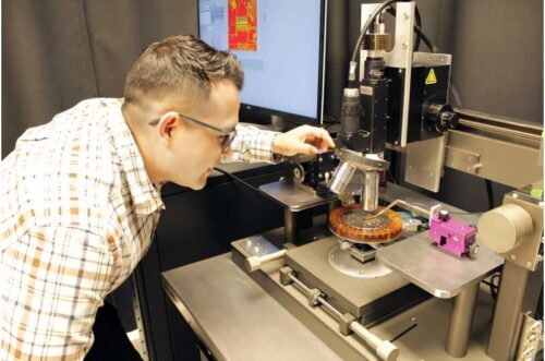
Nonetheless, UWBG semiconductors additionally include challenges. They’re costly, exhausting to fabricate, and tough to check for warmth buildup. As transistors shrink and extra energy is packed into smaller areas, warmth can accumulate in tiny zones—typically reaching vitality flux ranges greater than the floor of the solar. This creates a robust want for brand spanking new instruments that may precisely measure temperature at microscopic scales.
To deal with this, researchers are creating superior thermal metrology methods. Optical strategies like Raman spectroscopy and thermoreflectance use gentle to detect temperature. Electrical methods infer warmth from adjustments in voltage or resistance. Scanning-probe strategies—reminiscent of scanning thermal microscopy—bodily contact the floor to search out scorching spots. Hybrid approaches are additionally rising. These embrace combining multicolor thermal imaging to visualise nitride gadgets, monitoring defect-related absorption in gallium oxide elements, and utilizing deep-ultraviolet microscopes to map warmth patterns smaller than a micrometer.
Collectively, these new supplies and thermal instruments supply a path to smaller, extra environment friendly, and extra dependable electronics. They assist prolong gadget lifetimes, scale back vitality waste, and allow higher efficiency in harsh situations—paving the best way for advances throughout a number of industries.
