

The low-cost technique provides high-speed GaN transistors instantly to straightforward silicon chips for higher efficiency and simple scaling.
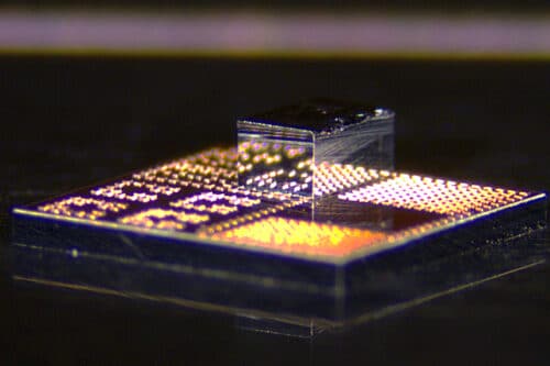
Researchers at MIT and accomplice establishments have developed a brand new course of to combine gallium nitride (GaN) transistors onto normal silicon CMOS chips. The method fabricates dense arrays of ultra-small GaN transistors—every solely 240 by 410 microns—on a GaN wafer. These are then laser-cut into particular person dielets.
Every dielet consists of copper pillars that bond on to matching copper options on a CMOS chip. A custom-built meeting device aligns the dielets utilizing vacuum management and nanometer-scale positioning earlier than bonding at temperatures beneath 400°C.

Not like conventional strategies that require solder or gold bonding, this strategy makes use of copper-to-copper bonding, which is extra suitable with normal semiconductor fabrication environments.
The researchers demonstrated this method by constructing energy amplifier chips on Intel 22nm FinFET-based silicon, exhibiting how GaN transistors may be added to superior digital platforms.
This course of eliminates the necessity to bond a complete GaN wafer to silicon, considerably lowering GaN materials utilization. Solely the mandatory transistors are transferred, minimizing waste and reducing materials prices.
Copper bonding at low temperatures avoids thermal injury to delicate parts and doesn’t require costly supplies like gold, which additionally pose contamination dangers in normal fabs.
The tactic helps high-density integration of GaN transistors with superior silicon nodes, permitting using extra circuit components like neutralization capacitors that enhance RF efficiency.
By becoming inside present chip manufacturing workflows, the method allows simpler scaling and industrial adoption with out main adjustments to fabrication infrastructure.
The ensuing chips are smaller, sooner, and extra environment friendly. Energy amplifiers made utilizing this technique ship larger bandwidth and stronger sign acquire in comparison with these made with silicon alone.
This integration method might result in improved wi-fi connectivity, longer battery life in cell units, and extra compact {hardware} design.
As a result of GaN performs higher than silicon at low temperatures, the identical technique might help rising functions equivalent to cryogenic electronics and quantum computing.
By bridging the strengths of GaN and silicon in a low-cost, scalable manner, the know-how opens new prospects for high-performance techniques—from cellphones to AI and next-generation communication infrastructure.
